Advanced PCB Design Software
CR-8000: Product-centric 3D PCB Design Platform
Building a competitive product today is much more difficult than a few years ago. Existing PCB-centric design processes are limited to a single PCB and do not provide the necessary tools for today’s competitive product development environment. PCB-centric design processes are falling behind.
CR-8000 is a product-centric design solution that provides the tools to optimize a design at both the product and PCB design level. Product-centric design processes provide architectural validation of the design against product requirements. Validating the product architecture against the product requirements significantly reduces delivery risk. Product-centric detailed design includes 2D/3D multi-board design and implementation, FPGA I/O optimization, chip/package/board co-design, and 3D MCAD integration all in one design process.
Take the CR-8000 Product Tour
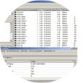 |
Multi-site ECAD Library & DataLibrary and data management needs to be scalable from one site to many. Designs and library data need to be versioned and all changes synchronized across your organization. |
 |
Design ExplorationDesign exploration and optimization bridges the design process gap between marketing requirements and detailed design. Bridging this gap will improve product quality, lower costs and delivery risk. |
|
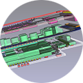 |
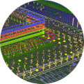
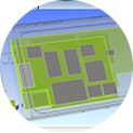
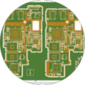
2D/3D Multi-board PCB DesignToday’s complex products require a new design approach where multiple boards can be managed as a single design with 2D and 3D visualization |
 |
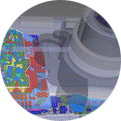
Advanced PackagingDesign Force offers an intuitive, integrated environment for designing single and multi-die packages for wire-bond, flip-chip, and high density advanced packaging or printed circuit board (PCB). |
|
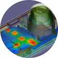 |
3D ECAD/MCAD Convergence3D product visualization is becoming a critical need as the electrical and mechanical designs converge with little room for error. Detection at the prototype phase may be too late. |
 |
Chip-Package-Board Co-designPoor I/O assignments on a newly designed package can leave a PCB unroutable. Merging the packaging and PCB design into a single design solution significantly increases design quality. |
|
 |
Modular DesignCompetitive products are combining the re-use of trusted design elements with new innovative design. Formal design reuse across your organization allows you to focus on innovation. |
 |
Simulation and AnalysisDuring circuit design, Design Gateway provides embedded simulation, analysis and electrical rules checking. |
|
 |
FPGA Pin OptimizationGraphical Pin Manager enables design teams to communicate I/O and constraint information intelligently for FPGAs or other high-pin count devices, at any time, using Design Gateway and Design Force. |
 |
Design for ManufacturingConduct manufacturing audits at any point in the design cycle and create manufacturing outputs for package, flex, or rigid designs. |